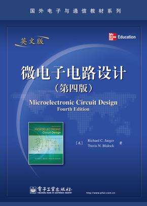
微电子电路设计(第四版)(英文版)"
本书涵盖了微电子电路设计所需基础知识,主要由三个部分组成。第一部分介绍固态电子学与器件,讨论了电子学的发展与电路分析方法和微电子器件的工作原理、I-V特性及SPICE模型等。第二部分为数字电路,包括数字电路的基本概念和CMOS电路、存储电路、ECL与TTL等双极型逻辑电路以及BiCMOS电路。第三部分为模拟电路,以理想运算放大器和SPICE仿真为基础介绍了不同结构运算放大器的相关特性、小信号模型、具体分析方法和集成设计技术,最后讨论了放大器的频率响应、反馈和振荡器等问题。 通过学习本书可以了解现代微电子电路设计,包括模拟与数字,分立与集成,了解内部结构也有利于系统设计中对集成电路的适当选择。 读者对象:本书适用作电子与信息类各专业本科生基础课的双语教材或参考书,也可作为相关领域工程技术人员的参考资料。
PREFACE Through study of this text, the reader will develop a com-prehensive understanding of the basic techniques of mod-ern electronic circuit design, analog and digital, discrete and integrated. Even though most readers may not ulti-mately be engaged in the design of integrated circuits (ICs) themselves, a thorough understanding of the internal circuit structure of ICs is prerequisite to avoiding many pitfalls that prevent the effective and reliable application of integrated circuits in system design. Digital electronics has evolved to be an extremely im-portant area of circuit design, but it is included almost as an afterthought in many introductory electronics texts. We present a more balanced coverage of analog and digital cir-cuits. The writing integrates the authors’ extensive indus-trial backgrounds in precision analog and digital design with their many years of experience in the classroom. A broad spectrum of topics is included, and material can easily be selected to satisfy either a two-semester or three-quarter sequence in electronics. IN THIS EDITION This edition continues to update the material to achieve improved readability and accessibility to the student. In addition to general material updates, a number of spe-ci.c changes have been included in Parts I and II, Solid-State Electronics and Devices and Digital Electronics, respectively. A new closed-form solution to four-resistor MOSFET biasing is introduced as well as an improved iterative strategy for diode Q-point analysis. JFET devices are important in analog design and have been reintro-duced at the end of Chapter 4. Simulation-based logic gate scaling is introduced in the MOS logic chapters, and an enhanced discussion of noise margin is included as a new Electronics-in-Action (EIA) feature. Current-mode logic (CML) is heavily used in high performance SiGe ICs, and a CML section is added to the Bipolar Logic chapter. This revision contains major reorganization and revi-sion of the analog portion (Part III) of the text. The introduc-tory ampli.er material (old Chapter 10) is now introduced xx in a “just-in-time” basis in the three op-amp chapters. Spe-ci.c sections have been added with qualitative descriptions of the operation of basic op-amp circuits and each transistor ampli.er con.guration as well as the transistors themselves. Feedback analysis using two-ports has been eliminated from Chapter 18 in favor of a consistent loop-gain analy-sis approach to all feedback con.gurations that begins in the op-amp chapters. The important successive voltage and current injection technique for .nding loop-gain is now in-cluded in Chapter 11, and Blackman’s theorem is utilized to .nd input and output resistances of closed-loop ampli.ers. SPICE examples have been modi.ed to utilize three-and .ve-terminal built-in op-amp models. Chapter 10, Analog Systems and Ideal Operational Ampli.ers, provides an introduction to ampli.ers and cov-ers the basic ideal op-amp circuits. Chapter 11, Characteristics and Limitations of Opera-tional Ampli.ers, covers the limitations of nonideal op amps including frequency response and stability and the four clas-sic feedback circuits including series-shunt, shunt-shunt, shunt-series and series-series feedback ampli.ers. Chapter 12, Operational Ampli.er Applications, col-lects together all the op-amp applications including multi-stage ampli.ers, .lters, A/D and D/A converters, sinusoidal oscillators, and multivibrators. Redundant material in transistor ampli.er chapters 13 and 14 has been merged or eliminated wherever possible. Other additions to the analog material include discussion of relations between MOS logic inverters and common-source ampli.ers, distortion reduction through feedback, the rela-tionship between step response and phase margin, NMOS differential ampli.ers with NMOS load transistors, the reg-ulated cascode current source, and the Gilbert multiplier. Because of the renaissance and pervasive use of RF circuits, the introductory section on RF ampli.ers, now in Chapter 17, has been expanded to include shunt-peaked and tuned ampli.ers, and the use of inductive degeneration in common-source ampli.ers. New material on mixers in-cludes passive, active, single-and double-balanced mixers and the widely used Gilbert mixer. Preface xxi Chapter 18, Transistor Feedback Ampli.ers and Oscillators, presents examples of transistor feedback am-pli.ers and transistor oscillator implementations. The tran-sistor oscillator section has been expanded to include a discussion of negative resistance in oscillators and the negative Gm oscillator cell. Several other important enhancements include: . SPICE support on the web now includes examples in NI Multisim. software in addition to PSpice.. . At least 35 percent revised or new problems. . New PowerPoint. slides are available from McGraw-Hill. . A group of tested design problems are also available. The Structured Problem Solving Approach continues to be utilized throughout the examples. We continue to expand the popular Electronics-in-Action Features with the addition of Diode Recti.er as an AM Demodulator; High Performance CMOS Technologies; A Second Look at Noise Margins (graphical .ip-.op approach); Offset Voltage, Bias Cur-rent and CMRR Measurement; Sample-and-Hold Circuits; Voltage Regulator with Series Pass Transistor; Noise Fac-tor, Noise Figure and Minimum Detectable Signal; Series-Parallel and Parallel-Series Network Transformations; and Passive Diode Ring Mixer. Chapter Openers enhance the readers understanding of historical developments in electronics. Design notes high-light important ideas that the circuit designer should re-member. The World Wide Web is viewed as an integral extension of the text, and a wide range of supporting mate-rials and resource links are maintained and updated on the McGraw-Hill website (www.mhhe.com/jaeger). Features of the book are outlined below. The Structured Problem-Solving Approach is used throughout the examples. Electronics-in-Action features in each chapter. Chapter openers highlighting developments in the .eld of electronics. Design Notes and emphasis on practical circuit design. Broad use of SPICE throughout the text and examples. Integrated treatment of device modeling in SPICE. Numerous Exercises, Examples, and Design Examples. Large number of new problems. Integrated web materials. Continuously updated web resources and links. Placing the digital portion of the book .rst is also bene-.cial to students outside of electrical engineering, partic-ularly computer engineering or computer science majors, who may only take the .rst course in a sequence of elec-tronics courses. The material in Part II deals primarily with the internal design of logic gates and storage elements. A comprehen-sive discussion of NMOS and CMOS logic design is pre-sented in Chapters 6 and 7, and a discussion of memory cells and peripheral circuits appears in Chapter 8. Chap-ter 9 on bipolar logic design includes discussion of ECL, CML and TTL. However, the material on bipolar logic has been reduced in deference to the import of MOS technol-ogy. This text does not include any substantial design at the logic block level, a topic that is fully covered in digital design courses. Parts I and II of the text deal only with the large-signal characteristics of the transistors. This allows readers to be-come comfortable with device behavior and i-v characteris-tics before they have to grasp the concept of splitting circuits into different pieces (and possibly different topologies) to perform dc and ac small-signal analyses. (The concept of a small-signal is formally introduced in Part III, Chapter 13.) Although the treatment of digital circuits is more ex-tensive than most texts, more than 50 percent of the mate-rial in the book, Part III, still deals with traditional analog circuits. The analog section begins in Chapter 10 with a discussion of ampli.er concepts and classic ideal op-amp circuits. Chapter 11 presents a detailed discussion of non-ideal op amps, and Chapter 12 presents a range of op-amp applications. Chapter 13 presents a comprehensive devel-opment of the small-signal models for the diode, BJT, and FET. The hybrid-pi model and pi-models for the BJT and FET are used throughout. Chapter 14 provides in-depth discussion of single-stage ampli.er design and multistage ac coupled ampli.ers. Coupling and bypass capacitor design is also covered in Chapter 14. Chapter 15 discusses dc coupled multistage ampli.ers and introduces prototypical op amp circuits. Chapter 16 continues with techniques that are important in IC design and studies the classic 741 operational ampli.er. Chapter 17 develops the high-frequency models for the transistors and presents a detailed discussion of analysis of high-frequency circuit behavior. The .nal chapter presents examples of transistor feedback ampli.ers. Discussion of feedback ampli.er stability and oscillators conclude the text. xxii Preface DESIGN Design remains a dif.cult issue in educating engineers. The use of the well-de.ned problem-solving methodology presented in this text can signi.cantly enhance the students ability to understand issues related to design. The design examples assist in building an understanding of the design process. Part II launches directly into the issues associated with the design of NMOS and CMOS logic gates. The effects of device and passive-element tolerances are dis-cussed throughout the text. In today’s world, low-power, low-voltage design, often supplied from batteries, is play-ing an increasingly important role. Logic design examples havemovedawayfrom5Vtolowerpower supply levels. The use of the computer, including MATLAB., spread-sheets, or standard high-level languages to explore design options is a thread that continues throughout the text. Methods for making design estimates and decisions are stressed throughout the analog portion of the text. Ex-pressions for ampli.er behavior are simpli.ed beyond the standard hybrid-pi model expressions whenever appropri-ate. For example, the expression for the voltage gain of an ampli.er in most texts is simply written as |Av|=gm RL , which tends to hide the power supply voltage as the funda-mental design variable. Rewriting this expression in approx- ~~ imate form as gm RL =10VCC for the BJT, or gm RL =VDD for the FET, explicitly displays the dependence of ampli.er design on the choice of power supply voltage and provides a simple .rst-order design estimate for the voltage gain of the common-emitter and common-source ampli.ers. The gain advantage of the BJT stage is also clear. These approxima-tion techniques and methods for performance estimation are included as often as possible. Comparisons and design tradeoffs between the properties of BJTs and FETs are in-cluded throughout Part III. Worst-case and Monte-Carlo analysis techniques are introduced at the end of the .rst chapter. These are not top-ics traditionally included in undergraduate courses. How-ever, the ability to design circuits in the face of wide component tolerances and variations is a key component of electronic circuit design, and the design of circuits using standard components and tolerance assignment are discussed in examples and included in many problems. PROBLEMS AND INSTRUCTOR SUPPORT Speci.c design problems, computer problems, and SPICE problems are included at the end of each chapter. Design problems are indicated by , computer problems are in-dicated by , and SPICE problems are indicated by . The problems are keyed to the topics in the text with the more dif.cult or time-consuming problems indicated by * and **. An Instructor’s Manual containing solutions to all the problems is available from the authors. In addition, the graphs and .gures are available as PowerPoint .les and can be retrieved from the website. Instructor notes are available as PowerPoint slides. ELECTRONIC TEXTBOOK OPTION This text is offered through CourseSmart for both instruc-tors and students. CourseSmart is an online resource where students can purchase the complete text online at almost half the cost of a traditional text. Purchasing the eTextbook al-lows students to take advantage of CourseSmart’s web tools for learning, which include full text search, notes and high-lighting, and email tools for sharing notes between class-mates. To learn more about CourseSmart options, contact your sales representative or visit www.CourseSmart.com. COSMOS Complete Online Solutions Manual Organization System (COSMOS). Professors can bene.t from McGraw-Hill’s COSMOS electronic solutions manual. COSMOS enables instructors to generate a limitless supply of problem mate-rial for assignment, as well as transfer and integrate their own problems into the software. For additional information, contact your McGraw-Hill sales representative. COMPUTER USAGE AND SPICE The computer is used as a tool throughout the text. The au-thors .rmly believe that this means more than just the use of the SPICE circuit analysis program. In today’s comput-ing environment, it is often appropriate to use the computer to explore a complex design space rather than to try to re-duce a complicated set of equations to some manageable analytic form. Examples of the process of setting up equa-tions for iterative evaluation by computer through the use of spreadsheets, MATLAB, and/or standard high-level lan-guage programs are illustrated in several places in the text. MATLAB is also used for Nyquist and Bode plot generation and is very useful for Monte Carlo analysis. On the other hand, SPICE is used throughout the text. Results from SPICE simulation are included throughout and numerous SPICE problems are to be found in the problem sets. Wherever helpful, a SPICE analysis is used with most examples. This edition also emphasizes the dif-ferences and utility of the dc, ac, transient, and transfer function analysis modes in SPICE. A discussion of SPICE device modeling is included following the introduction to each semiconductor device, and typical SPICE model parameters are presented with the models. ACKNOWLEDGMENTS We want to thank the large number of people who have had an impact on the material in this text and on its prepara-tion. Our students have helped immensely in polishing the manuscript and have managed to survive the many revi-sions of the manuscript. Our department heads, J. D. Irwin of Auburn University and L. R. Harriott of the University of Virginia, have always been highly supportive of faculty efforts to develop improved texts. We want to thank all the reviewers and survey respon-dents including Vijay K. Arora Anthony Johnson Wilkes University The University of Toledo Kurt Behpour Marian K. Kazimierczuk California Polytechnic Wright State University State University, G. Roientan Lahiji San Luis Obispo Professor, Iran University David A. Borkholder of Science and Rochester Institute of Technology Technology Adjunct Professor, Dmitri Donetski University of Michigan Stony Brook University Stanislaw F. Legowski Ethan Farquhar University of Wyoming The University of Tennessee, Milica Markovic Knoxville California State University Melinda Holtzman Sacramento Portland State University Preface xxiii James E. Morris Kenneth V. Noren Portland State University University of Idaho Maryam Moussavi John Ortiz California State University University of Texas at Long Beach San Antonio We are also thankful for inspiration from the classic text Applied Electronics by J. F. Pierce and T. J. Paulus. Professor Blalock learned electronics from Professor Pierce many years ago and still appreciates many of the analytical techniques employed in their long out-of-print text. We would like to thank Gabriel Chindris of Technical University of Cluj-Napoca in Romania for his assistance in creating the simulations for the NI MultisimTM examples. Finally, we want to thank the team at McGraw-Hill including Raghothaman Srinivasan, Global Publisher; Darlene Schueller, Developmental Editor; Curt Reynolds, Senior Marketing Manager; Jane Mohr, Senior Project Man-ager; Brenda Rolwes, Design Coordinator; John Leland and LouAnn Wilson, Photo Research Coordinators; Kara Ku-dronowicz, Senior Production Supervisor; Sandy Schnee, Senior Media Project Manager; and Dheeraj Chahal, Full Service Project Manager, MPS Limited. In developing this text, we have attempted to integrate our industrial backgrounds in precision analog and digital design with many years of experience in the classroom. We hope we have at least succeeded to some extent. Construc-tive suggestions and comments will be appreciated. Richard C. Jaeger Auburn University Travis N. Blalock University of Virginia CHAPTER-BY-CHAPTER SUMMARY PART I—SOLID-STATE ELECTRONICS AND DEVICES Chapter 1 provides a historical perspective on the .eld of electronics beginning with vacuum tubes and advancing to giga-scale integration and its impact on the global economy. Chapter 1 also provides a classi.cation of electronic signals and a review of some important tools from network anal-ysis, including a review of the ideal operational ampli.er. Because developing a good problem-solving methodology is of such import to an engineer’s career, the comprehen-sive Structured Problem Solving Approach is used to help the students develop their problem solving skills. The struc-tured approach is discussed in detail in the .rst chapter and used in all the subsequent examples in the text. Component tolerances and variations play an extremely important role in practical circuit design, and Chapter 1 closes with intro-ductions to tolerances, temperature coef.cients, worst-case design, and Monte Carlo analysis. Chapter 2 deviates from the recent norm and discusses semiconductor materials including the covalent-bond and energy-band models of semiconductors. The chapter in-cludes material on intrinsic carrier density, electron and hole populations, n-and p-type material, and impurity doping. Mobility, resistivity, and carrier transport by both drift and diffusion are included as topics. Velocity saturation is dis-cussed, and an introductory discussion of microelectronic fabrication has been merged with Chapter 2. Chapter 3 introduces the structure and i-v character-istics of solid-state diodes. Discussions of Schottky diodes, variable capacitance diodes, photo-diodes, solar cells, and LEDs are also included. This chapter introduces the con-cepts of device modeling and the use of different levels of modeling to achieve various approximations to reality. The SPICE model for the diode is discussed. The con-cepts of bias, operating point, and load-line are all intro-duced, and iterative mathematical solutions are also used to .nd the operating point with MATLAB and spreadsheets. Diode applications in recti.ers are discussed in detail and a xxiv discussion of the dynamic switching characteristics of diodes is also presented. Chapter 4 discusses MOS and junction .eld-effect transistors, starting with a qualitative description of the MOS capacitor. Models are developed for the FET i-v char-acteristics, and a complete discussion of the regions of op-eration of the device is presented. Body effect is included. MOS transistor performance limits including scaling, cut-off frequency, and subthreshold conduction are discussed as well as basic A-based layout methods. Biasing circuits and load-line analysis are presented. The FET SPICE models and model parameters are discussed in Chapter 4. Chapter 5 introduces the bipolar junction transistor and presents a heuristic development of the Transport (sim-pli.ed Gummel-Poon) model of the BJT based upon su-perposition. The various regions of operation are discussed in detail. Common-emitter and common-base current gains are de.ned, and base transit-time, diffusion capacitance and cutoff frequency are all discussed. Bipolar technology and physical structure are introduced. The four-resistor bias cir-cuit is discussed in detail. The SPICE model for the BJT and the SPICE model parameters are discussed in Chapter 5. PART II—DIGITAL ELECTRONICS Chapter 6 begins with a compact introduction to digital electronics. Terminology discussed includes logic levels, noise margins, rise-and-fall times, propagation delay, fan out, fan in, and power-delay product. A short review of Boolean algebra is included. The introduction to MOS logic design is now merged with Chapter 6 and follows the histor-ical evolution of NMOS logic gates focusing on the design of saturated-load, and depletion-load circuit families. The impact of body effect on MOS logic circuit design is dis-cussed in detail. The concept of reference inverter scaling is developed and employed to affect the design of other in-verters, NAND gates, NOR gates, and complex logic func-tions throughout Chapters 6 and 7. Capacitances in MOS Chapter-by-Chapter Summary circuits are discussed, and methods for estimating the prop-agation delay and power-delay product of NMOS logic are presented. Details of several of the propagation delay anal-yses are moved to the MCD website, and the delay equation results for the various families have been collapsed into a much more compact form. The pseudo NMOS logic gate is discussed and provides a bridge to CMOS logic in Chapter 7. CMOS represents today’s most important integrated circuit technology, and Chapter 7 provides an in-depth look at the design of CMOS logic gates including invert-ers, NAND and NOR gates, and complex logic gates. The CMOS designs are based on simple scaling of a reference inverter design. Noise margin and latchup are discussed as well as a comparison of the power-delay products of vari-ous MOS logic families. Dynamic logic circuits and cascade buffer design are discussed in Chapter 7. A discussion of BiCMOS logic circuitry has been added to Chapter 9 after bipolar logic is introduced. Chapter 8 ventures into the design of memory and storage circuits, including the six-transistor, four-transistor, and one-transistor memory cells. Basic sense-ampli.er cir-cuits are introduced as well as the peripheral address and decoding circuits needed in memory designs. ROMs and .ip-.op circuitry are included in Chapter 8. Chapter 9 discusses bipolar logic circuits including emitter-coupled logic and transistor-transistor logic. The use of the differential pair as a current switch and the large-signal properties of the emitter follower are introduced. An introduction to CML, widely used in SiGe design, follows the ECL discussion. Operation of the BJT as a saturated switch is included and followed by a discussion of low volt-age and standard TTL. An introduction to BiCMOS logic now concludes the chapter on bipolar logic. PART III—ANALOG ELECTRONICS Chapter 10 provides a succinct introduction to analog elec-tronics. The concepts of voltage gain, current gain, power gain, and distortion are developed and have been merged on a “just-in-time” basic with the discussion of the classic ideal operational ampli.er circuits that include the invert-ing, noninverting, summing, and difference ampli.ers and the integrator and differentiator. Much care has been taken to be consistent in the use of the notation that de.nes these quantities as well as in the use of dc, ac, and total signal notation throughout the book. Bode plots are reviewed and ampli.ers are classi.ed by frequency response. MATLAB is utilized as a tool for producing Bode plots. SPICE simu-lation using built-in SPICE models is introduced. Chapter 11 focuses on a comprehensive discussion of the characteristics and limitations of real operational am-pli.ers including the effects of .nite gain and input resis-tance, nonzero output resistance, input offset voltage, input bias and offset currents, output voltage and current limits, .nite bandwidth, and common-mode rejection. A consis-tent loop-gain analysis approach is used to study the four classic feedback con.gurations, and Blackman’s theorem is utilized to .nd input and output resistances of closed-loop ampli.ers. The important successive voltage and current injection technique for .nding loop-gain is now included in Chapter 11. Relationships between the Nyquist and Bode techniques are explicitly discussed. Stability of .rst-, second-and third-order systems is discussed, and the con-cepts of phase and gain margin are introduced. Relation-ships between Nyquist and Bode techniques are explicitly discussed. A section concerning the relationship between phase margin and time domain response has been added. The macro model concept is introduced and the discussion of SPICE simulation of op-amp circuits using various levels of models continues in Chapter 11. Chapter 12 covers a wide range of operational am-pli.er applications that include multistage ampli.ers, the instrumentation ampli.er, and continuous time and discrete time active .lters. Cascade ampli.ers are investigated in-cluding a discussion of the bandwidth of multistage ampli-.ers. An introduction to D/A and A/D converters appears in this chapter. The Barkhausen criterion for oscillation are presented and followed by a discussion of op-amp-based si-nusoidal oscillators. Nonlinear circuits applications includ-ing recti.ers, Schmitt triggers, and multivibrators conclude the material in Chapter 12. Chapter 13 begins the general discussion of linear ampli.cation using the BJT and FET as C-E and C-S am-pli.ers. Biasing for linear operation and the concept of small-signal modeling are both introduced, and small-signal models of the diode, BJT, and FET are all developed. The limits for small-signal operation are all carefully de.ned. The use of coupling and bypass capacitors and inductors to separate the ac and dc designs is explored. The impor-tant 10VCC and VDD design estimates for the voltage gain of the C-E and C-S ampli.ers are introduced, and the role of transistor ampli.cation factor in bounding circuit perfor-mance is discussed. The role of Q-point design on power dissipation and signal range is also introduced. Chapter 14 proceeds with an in-depth comparison of the characteristics of single-transistor ampli.ers, in-cluding small-signal amplitude limitations. Appropriate points for signal injection and extraction are identi.ed, and ampli.ers are classi.ed as inverting ampli.ers (C-E, C-S), noninverting ampli.ers (C-B, C-G), and followers (C-C, C-D). The treatment of MOS and bipolar devices is merged from Chapter 14 on, and design tradeoffs between xxvi Chapter-by-Chapter Summary the use of the BJT and the FET in ampli.er circuits is an important thread that is followed through all of Part III. A detailed discussion of the design of coupling and bypass capacitors and the role of these capacitors in controlling the low frequency response of ampli.ers appears in this chapter. Chapter 15 explores the design of multistage direct coupled ampli.ers. An evolutionary approach to multistage op amp design is used. MOS and bipolar differential ampli-.ers are .rst introduced. Subsequent addition of a second gain stage and then an output stage convert the differential ampli.ers into simple op amps. Class A, B, and AB oper-ation are de.ned. Electronic current sources are designed and used for biasing of the basic operational ampli.ers. Dis-cussion of important FET-BJT design tradeoffs are included wherever appropriate. Chapter 16 introduces techniques that are of particu-lar import in integrated circuit design. A variety of current mirror circuits are introduced and applied in bias circuits and as active loads in operational ampli.ers. A wealth of circuits and analog design techniques are explored through the detailed analysis of the classic 741 operational ampli-.er. The bandgap reference and Gilbert analog multiplier are introduced in Chapter 16. Chapter 17 discusses the frequency response of ana-log circuits. The behavior of each of the three categories of single-stage ampli.ers (C-E/C-S, C-B/C-G, and C-C/C-D) is discussed in detail, and BJT behavior is contrasted with that of the FET. The frequency response of the transistor is discussed, and the high frequency, small-signal models are developed for both the BJT and FET. Miller multipli-cation is used to obtain estimates of the lower and upper cutoff frequencies of complex multistage ampli.ers. Gain-bandwidth products and gain-bandwidth tradeoffs in design are discussed. Cascode ampli.er frequency response, and tuned ampli.ers are included in this chapter. Because of the renaissance and pervasive use of RF circuits, the introductory section on RF ampli.ers has been expanded to include shunt-peaked and tuned ampli.ers, and the use of inductive degeneration in common-source ampli-.ers. New material on mixers includes passive and active single-and double-balanced mixers and the widely used Gilbert mixer. Chapter 18 presents detailed examples of feedback as applied to transistor ampli.er circuits. The loop-gain analysis approach introduced in Chapter 11 is used to .nd the closed-loop ampli.er gain of various ampli.ers, and Blackman’s theorem is utilized to .nd input and output resistances of closed-loop ampli.ers. Ampli.er stability is also discussed in Chapter 18, and Nyquist diagrams and Bode plots (with MATLAB) are used to explore the phase and gain margin of ampli.ers. Ba-sic single-pole op amp compensation is discussed, and the unity gain-bandwidth product is related to ampli.er slew rate. Design of op amp compensation to achieve a desired phase margin is discussed. The discussion of transistor os-cillator circuits includes the Colpitts, Hartley and negative Gm con.gurations. Crystal oscillators are also discussed. Three Appendices include tables of standard compo-nent values (Appendix A), summary of the device models and sample SPICE parameters (Appendix B) and review of two-port networks (Appendix C). Data sheets for repre-sentative solid-state devices and operational ampli.ers are available via the WWW. Flexibility The chapters are designed to be used in a variety of differ-ent sequences, and there is more than enough material for a two-semester or three-quarter sequence in electronics. One can obviously proceed directly through the book. On the other hand, the material has been written so that the BJT chapter can be used immediately after the diode chapter if so desired (i.e., a 1-2-3-5-4 chapter sequence). At the present time, the order actually used at Auburn University is: 1. Introduction 2. Solid-State Electronics 3. Diodes 4. FETs 6. Digital Logic 7. CMOS Logic 8. Memory 5. The BJT 9. Bipolar Logic 10–18. Analog in sequence The chapters have also been written so that Part II, Digital Electronics, can be skipped, and Part III, Analog Electron-ics, can be used directly after completion of the coverage of the solid-state devices in Part I. If so desired, many of the quantitative details of the material in Chapter 2 may be skipped. In this case, the sequence would be 1.Introduction 2.Solid-State Electronics 3.Diodes 4.FETs 5.The BJT 10–18. Analog in sequence


CONTENTS Preface xx PART ONE SOLID STATE ELECTRONIC AND DEVICES 1 CHAPTER 1 INTRODUCTION TO ELECTRONICS 3 1.1 A Brief History of Electronics: From Vacuum Tubes to Giga-Scale Integration 5 1.2 Classification of Electronic Signals 8 1.2.1 Digital Signals 9 1.2.2 Analog Signals 9 1.2.3 A/D and D/A Converters—Bridging the Analog and Digital Domains 10 1.3 Notational Conventions 12 1.4 Problem-Solving Approach 13 1.5 Important Concepts from Circuit Theory 15 1.5.1 Voltage and Current Division 15 1.5.2 Th′ evenin and Norton Circuit Representations 16 1.6 Frequency Spectrum of Electronic Signals 21 1.7 Amplifiers 22 1.7.1 Ideal Operational Amplifiers 23 1.7.2 Amplifier Frequency Response 25 1.8 Element Variations in Circuit Design 26 1.8.1 Mathematical Modeling of Tolerances 26 1.8.2 Worst-Case Analysis 27 1.8.3 Monte Carlo Analysis 29 1.8.4 Temperature Coefficients 32 1.9 Numeric Precision 34 Summary 34 Key Terms 35 References 36 Additional Reading 36 Problems 37 CHAPTER 2 SOLID-STATE ELECTRONICS 42 2.1 Solid-State Electronic Materials 44 2.2 Covalent Bond Model 45 2.3 Drift Currents and Mobility in Semiconductors 48 2.3.1 Drift Currents 48 2.3.2 Mobility 49 2.3.3 Velocity Saturation 49 2.4 Resistivity of Intrinsic Silicon 50 2.5 Impurities in Semiconductors 51 2.5.1 Donor Impurities in Silicon 52 2.5.2 Acceptor Impurities in Silicon 52 2.6 Electron and Hole Concentrations in Doped Semiconductors 52 2.6.1 n-Type Material (ND >NA ) 53 2.6.2 p-Type Material (NA >ND ) 54 2.7 Mobility and Resistivity in Doped Semiconductors 55 2.8 Diffusion Currents 59 2.9 Total Current 60 2.10 Energy Band Model 61 2.10.1 Electron–Hole Pair Generation in an Intrinsic Semiconductor 61 2.10.2 Energy Band Model for a Doped Semiconductor 62 2.10.3 Compensated Semiconductors 62 2.11 Overview of Integrated Circuit Fabrication 64 Summary 67 Key Terms 68 Reference 69 Additional Reading 69 Important Equations 69 Problems 70 CHAPTER 3 SOLID-STATE DIODES AND DIODE CIRCUITS 74 3.1 The pn Junction Diode 75 3.1.1 pn Junction Electrostatics 75 3.1.2 Internal Diode Currents 79 viii Contents 3.2 The i-v Characteristics of the Diode 80 3.14 Full-Wave Rectifier Circuits 123 3.3 The Diode Equation: A Mathematical Model 3.14.1 Full-Wave Rectifier with Negative for the Diode 82 Output Voltage 124 3.4 Diode Characteristics Under Reverse, Zero, 3.15 Full-Wave Bridge Rectification 125 and Forward Bias 85 3.16 Rectifier Comparison and Design 3.4.1 Reverse Bias 85 Tradeoffs 125 3.4.2 Zero Bias 85 3.17 Dynamic Switching Behavior of the 3.4.3 Forward Bias 86 Diode 129 3.5 Diode Temperature Coefficient 89 3.18 Photo Diodes, Solar Cells, and 3.6 Diodes Under Reverse Bias 89 Light-Emitting Diodes 130 3.6.1 Saturation Current in Real 3.18.1 Photo Diodes and Diodes 90 Photodetectors 130 3.6.2 Reverse Breakdown 91 3.18.2 Power Generation from Solar 3.6.3 Diode Model for the Breakdown Cells 131 Region 92 3.18.3 Light-Emitting Diodes (LEDs) 132 3.7 pn Junction Capacitance 92 Summary 133 3.7.1 Reverse Bias 92 Key Terms 134 3.7.2 Forward Bias 93 Reference 135 3.8 Schottky Barrier Diode 93 Additional Reading 135 3.9 Diode SPICE Model and Layout 94 Problems 135 3.10 Diode Circuit Analysis 96 3.10.1 Load-Line Analysis 96 CHAPTER 4 3.10.2 Analysis Using the Mathematical FIELD-EFFECT TRANSISTORS 145 Model for the Diode 98 3.10.3 The Ideal Diode Model 102 4.1 Characteristics of the MOS Capacitor 146 3.10.4 Constant Voltage Drop Model 104 4.1.1 Accumulation Region 147 3.10.5 Model Comparison and 4.1.2 Depletion Region 148 Discussion 105 4.1.3 Inversion Region 148 3.11 Multiple-Diode Circuits 106 4.2 The NMOS Transistor 148 3.12 Analysis of Diodes Operating in the 4.2.1 Qualitative i -v Behavior of the Breakdown Region 109 NMOS Transistor 149 3.12.1 Load-Line Analysis 109 4.2.2 Triode Region Characteristics of the 3.12.2 Analysis with the Piecewise Linear NMOS Transistor 150 Model 109 4.2.3 On Resistance 153 3.12.3 Voltage Regulation 110 4.2.4 Saturation of the i -v 3.12.4 Analysis Including Zener Characteristics 154 Resistance 111 4.2.5 Mathematical Model in the 3.12.5 Line and Load Regulation 112 Saturation (Pinch-Off) Region 155 3.13 Half-Wave Rectifier Circuits 113 4.2.6 Transconductance 157 3.13.1 Half-Wave Rectifier with Resistor 4.2.7 Channel-Length Modulation 157 Load 113 4.2.8 Transfer Characteristics and 3.13.2 Rectifier Filter Capacitor 114 Depletion-Mode MOSFETS 158 3.13.3 Half-Wave Rectifier with RC 4.2.9 Body Effect or Substrate Load 115 Sensitivity 159 3.13.4 Ripple Voltage and Conduction 4.3 PMOS Transistors 161 Interval 116 4.4 MOSFET Circuit Symbols 163 3.13.5 Diode Current 118 4.5 Capacitances in MOS Transistors 165 3.13.6 Surge Current 120 4.5.1 NMOS Transistor Capacitances in 3.13.7 Peak-Inverse-Voltage (PIV) the Triode Region 165 Rating 120 4.5.2 Capacitances in the Saturation 3.13.8 Diode Power Dissipation 120 Region 166 3.13.9 Half-Wave Rectifier with Negative 4.5.3 Capacitances in Cutoff 166 Output Voltage 121 4.6 MOSFET Modeling in SPICE 167 Contents ix 4.7 MOS Transistor Scaling 169 4.7.1 Drain Current 169 4.7.2 Gate Capacitance 169 4.7.3 Circuit and Power Densities 170 4.7.4 Power-Delay Product 170 4.7.5 Cutoff Frequency 171 4.7.6 High Field Limitations 171 4.7.7 Subthreshold Conduction 172 4.8 MOS Transistor Fabrication and Layout Design Rules 172 4.8.1 Minimum Feature Size and Alignment Tolerance 173 4.8.2 MOS Transistor Layout 173 4.9 Biasing the NMOS Field-Effect Transistor 176 4.9.1 Why Do We Need Bias? 176 4.9.2 Constant Gate-Source Voltage Bias 178 4.9.3 Load Line Analysis for the Q-Point 181 4.9.4 Four-Resistor Biasing 182 4.10 Biasing the PMOS Field-Effect Transistor 188 4.11 The Junction Field-Effect Transistor (JFET) 190 4.11.1 The JFET with Bias Applied 191 4.11.2 JFET Channel with Drain-Source Bias 191 4.11.3 n-Channel JFET i -v Characteristics 193 4.11.4 The p-Channel JFET 195 4.11.5 Circuit Symbols and JFET Model Summary 195 4.11.6 JFET Capacitances 196 4.12 JFET Modeling in SPICE 197 4.13 Biasing the JFET and Depletion-Mode MOSFET 198 Summary 200 Key Terms 202 References 203 Problems 204 CHAPTER 5 BIPOLAR JUNCTION TRANSISTORS 217 5.1 Physical Structure of the Bipolar Transistor 218 5.2 The Transport Model for the npn Transistor 219 5.2.1 Forward Characteristics 220 5.2.2 Reverse Characteristics 222 5.2.3 The Complete Transport Model Equations for Arbitrary Bias Conditions 223 5.3 The pnp Transistor 225 5.4 Equivalent Circuit Representations for the Transport Models 227 5.5 The i-v Characteristics of the Bipolar Transistor 228 5.5.1 Output Characteristics 228 5.5.2 Transfer Characteristics 229 5.6 The Operating Regions of the Bipolar Transistor 230 5.7 Transport Model Simplifications 231 5.7.1 Simplified Model for the Cutoff Region 231 5.7.2 Model Simplifications for the Forward-Active Region 233 5.7.3 Diodes in Bipolar Integrated Circuits 239 5.7.4 Simplified Model for the Reverse-Active Region 240 5.7.5 Modeling Operation in the Saturation Region 242 5.8 Nonideal Behavior of the Bipolar Transistor 245 5.8.1 Junction Breakdown Voltages 246 5.8.2 Minority-Carrier Transport in the Base Region 246 5.8.3 Base Transit Time 247 5.8.4 Diffusion Capacitance 249 5.8.5 Frequency Dependence of the Common-Emitter Current Gain 250 5.8.6 The Early Effect and Early Voltage 250 5.8.7 Modeling the Early Effect 251 5.8.8 Origin of the Early Effect 251 5.9 Transconductance 252 5.10 Bipolar Technology and SPICE Model 253 5.10.1 Qualitative Description 253 5.10.2 SPICE Model Equations 254 5.10.3 High-Performance Bipolar Transistors 255 5.11 Practical Bias Circuits for the BJT 256 5.11.1 Four-Resistor Bias Network 258 5.11.2 Design Objectives for the Four-Resistor Bias Network 260 5.11.3 Iterative Analysis of the Four-Resistor Bias Circuit 266 5.12 Tolerances in Bias Circuits 266 5.12.1 Worst-Case Analysis 267 5.12.2 Monte Carlo Analysis 269 Summary 272 Key Terms 274 References 274 Problems 275 x Contents PART TWO 6.11.1 Capacitances in Logic Circuits 337 6.11.2 Dynamic Response of the NMOS DIGITAL ELECTRONICS 285 Inverter with a Resistive Load 338 6.11.3 Pseudo NMOS Inverter 343 CHAPTER 6 6.11.4 A Final Comparison of NMOS INTRODUCTION TO DIGITAL ELECTRONICS 287 Inverter Delays 344 6.11.5 Scaling Based Upon Reference 6.1 Ideal Logic Gates 289 Circuit Simulation 3466.2 Logic Level Definitions and Noise 6.11.6 Ring Oscillator Measurement of Margins 289 Intrinsic Gate Delay 346 6.2.1 Logic Voltage Levels 291 6.11.7 Unloaded Inverter Delay 347 6.2.2 Noise Margins 291 6.12 PMOS Logic 349 6.2.3 Logic Gate Design Goals 292 6.12.1 PMOS Inverters 3496.3 Dynamic Response of Logic Gates 293 6.12.2 NOR and NAND Gates 352 6.3.1 Rise Time and Fall Time 293 Summary 352 6.3.2 Propagation Delay 294 Key Terms 354 6.3.3 Power-Delay Product 294 References 355 6.4 Review of Boolean Algebra 295 Additional Reading 355 6.5 NMOS Logic Design 297 Problems 355 6.5.1 NMOS Inverter with Resistive Load 298 CHAPTER 7 6.5.2 Design of the W/L Ratio of MS 299 6.5.3 Load Resistor Design 300 COMPLEMENTARY MOS (CMOS) LOGIC 6.5.4 Load-Line Visualization 300 DESIGN 367 6.5.5 On-Resistance of the Switching 7.1 CMOS Inverter Technology 368Device 302 7.1.1 CMOS Inverter Layout 370 6.5.6 Noise Margin Analysis 303 7.2 Static Characteristics of the CMOS 6.5.7 Calculation of VIL and VOH 303 Inverter 370 6.5.8 Calculation of VIH and VOL 304 7.2.1 CMOS Voltage Transfer 6.5.9 Load Resistor Problems 305 Characteristics 371 6.6 Transistor Alternatives to the Load 7.2.2 Noise Margins for the CMOS Resistor 306 Inverter 373 6.6.1 The NMOS Saturated Load 7.3 Dynamic Behavior of the CMOS Inverter 375 Inverter 307 7.3.1 Propagation Delay Estimate 375 6.6.2 NMOS Inverter with a Linear Load 7.3.2 Rise and Fall Times 377Device 315 7.3.3 Performance Scaling 377 6.6.3 NMOS Inverter with a 7.3.4 Delay of Cascaded Inverters 379Depletion-Mode Load 316 7.4 Power Dissipation and Power Delay Product 6.6.4 Static Design of the Pseudo NMOS in CMOS 380 Inverter 319 7.4.1 Static Power Dissipation 3806.7 NMOS Inverter Summary and 7.4.2 Dynamic Power Dissipation 381Comparison 323 7.4.3 Power-Delay Product 3826.8 NMOS NAND and NOR Gates 324 7.5 CMOS NOR and NAND Gates 384 6.8.1 NOR Gates 325 7.5.1 CMOS NOR Gate 384 6.8.2 NAND Gates 326 7.5.2 CMOS NAND Gates 387 6.8.3 NOR and NAND Gate Layouts in 7.6 Design of Complex Gates in CMOS 388NMOS Depletion-Mode 7.7 Minimum Size Gate Design and Technology 327 Performance 393 6.9 Complex NMOS Logic Design 328 7.8 Dynamic Domino CMOS Logic 3956.10 Power Dissipation 333 7.9 Cascade Buffers 397 6.10.1 Static Power Dissipation 333 7.9.1 Cascade Buffer Delay Model 397 6.10.2 Dynamic Power Dissipation 334 7.9.2 Optimum Number of Stages 398 6.10.3 Power Scaling in MOS Logic 7.10 The CMOS Transmission Gate 400Gates 335 7.11 CMOS Latchup 4016.11 Dynamic Behavior of MOS Logic Gates 337 Contents xi Summary 404 9.1.2 Current Switch Analysis for Key Terms 405 vI > VREF 463 References 406 9.1.3 Current Switch Analysis for Problems 406 vI < VREF 464 9.2 The Emitter-Coupled Logic (ECL) Gate 464 CHAPTER 8 9.2.1 ECL Gate with vI = VH 465 9.2.2 ECL Gate with vI = VL 466 MOS MEMORY AND STORAGE CIRCUITS 416 9.2.3 Input Current of the ECL Gate 466 8.1 Random Access Memory 417 9.2.4 ECL Summary 466 8.1.1 Random Access Memory (RAM) 9.3 Noise Margin Analysis for the ECL Gate 467 Architecture 417 9.3.1 VIL , VOH , VIH , and VOL 467 8.1.2 A 256-Mb Memory Chip 418 9.3.2 Noise Margins 468 8.2 Static Memory Cells 419 9.4 Current Source Implementation 469 8.2.1 Memory Cell Isolation and 9.5 The ECL OR-NOR Gate 471 Access—The 6-T Cell 422 9.6 The Emitter Follower 473 8.2.2 The Read Operation 422 9.6.1 Emitter Follower with a Load 8.2.3 Writing Data into the 6-T Cell 426 Resistor 474 8.3 Dynamic Memory Cells 428 9.7 “Emitter Dotting’’ or “Wired-OR’’ Logic 476 8.3.1 The One-Transistor Cell 430 9.7.1 Parallel Connection of 8.3.2 Data Storage in the 1-T Cell 430 Emitter-Follower Outputs 477 8.3.3 Reading Data from the 1-T Cell 431 9.7.2 The Wired-OR Logic Function 477 8.3.4 The Four-Transistor Cell 433 9.8 ECL Power-Delay Characteristics 477 8.4 Sense Amplifiers 434 9.8.1 Power Dissipation 477 8.4.1 A Sense Amplifier for the 6-T 9.8.2 Gate Delay 479 Cell 434 9.8.3 Power-Delay Product 480 8.4.2 A Sense Amplifier for the 1-T 9.9 Current Mode Logic 481 Cell 436 9.9.1 CML Logic Gates 481 8.4.3 The Boosted Wordline Circuit 438 9.9.2 CML Logic Levels 482 8.4.4 Clocked CMOS Sense 9.9.3 VEE Supply Voltage 482 Amplifiers 438 9.9.4 Higher-Level CML 483 8.5 Address Decoders 440 9.9.5 CML Power Reduction 484 8.5.1 NOR Decoder 440 9.9.6 NMOS CML 485 8.5.2 NAND Decoder 440 9.10 The Saturating Bipolar Inverter 487 8.5.3 Decoders in Domino CMOS 9.10.1 Static Inverter Characteristics 488 Logic 443 9.10.2 Saturation Voltage of the Bipolar 8.5.4 Pass-Transistor Column Transistor 488 Decoder 443 9.10.3 Load-Line Visualization 491 8.6 Read-Only Memory (ROM) 444 9.10.4 Switching Characteristics of the 8.7 Flip-Flops 447 Saturated BJT 491 8.7.1 RS Flip-Flop 449 9.11 A Transistor-Transistor Logic (TTL) 8.7.2 The D-Latch Using Transmission Prototype 494 Gates 450 9.11.1 TTL Inverter for vI = VL 494 8.7.3 A Master-Slave D Flip-Flop 450 9.11.2 TTL Inverter for vI = VH 495 Summary 451 9.11.3 Power in the Prototype TTL Key Terms 452 Gate 496 References 452 9.11.4 VIH , VIL, and Noise Margins for the Problems 453 TTL Prototype 496 9.11.5 Prototype Inverter Summary 498 9.11.6 Fanout Limitations of the TTL CHAPTER 9 Prototype 498 BIPOLAR LOGIC CIRCUITS 460 9.12 The Standard 7400 Series TTL Inverter 500 9.1 The Current Switch (Emitter-Coupled 9.12.1 Analysis for vI = VL 500 Pair) 461 9.12.2 Analysis for vI = VH 501 9.1.1 Mathematical Model for Static Behavior of the Current Switch 462 xii Contents 9.12.3 Power Consumption 503 9.12.4 TTL Propagation Delay and Power-Delay Product 503 9.12.5 TTL Voltage Transfer Characteristic and Noise Margins 503 9.12.6 Fanout Limitations of Standard TTL 504 9.13 Logic Functions in TTL 504 9.13.1 Multi-Emitter Input Transistors 505 9.13.2 TTL NAND Gates 505 9.13.3 Input Clamping Diodes 506 9.14 Schottky-Clamped TTL 506 9.15 Comparison of the Power-Delay Products of ECL and TTL 508 9.16 BiCMOS Logic 508 9.16.1 BiCMOS Buffers 509 9.16.2 BiNMOS Inverters 511 9.16.3 BiCMOS Logic Gates 513 Summary 513 Key Terms 515 References 515 Additional Reading 515 Problems 516 PART THREE ANALOG ELECTRONICS 527 CHAPTER 10 ANALOG SYSTEMS AND IDEAL OPERATIONAL AMPLIFIERS 529 10.1 An Example of an Analog Electronic System 530 10.2 Amplification 531 10.2.1 Voltage Gain 532 10.2.2 Current Gain 533 10.2.3 Power Gain 533 10.2.4 The Decibel Scale 534 10.3 Two-Port Models for Amplifiers 537 10.3.1 The g-parameters 537 10.4 Mismatched Source and Load Resistances 541 10.5 Introduction to Operational Amplifiers 544 10.5.1 The Differential Amplifier 544 10.5.2 Differential Amplifier Voltage Transfer Characteristic 545 10.5.3 Voltage Gain 545 10.6 Distortion in Amplifiers 548 10.7 Differential Amplifier Model 549 10.8 Ideal Differential and Operational Amplifiers 551 10.8.1 Assumptions for Ideal Operational Amplifier Analysis 551 10.9 Analysis of Circuits Containing Ideal Operational Amplifiers 552 10.9.1 The Inverting Amplifier 553 10.9.2 The Transresistance Amplifier—A Current-to-Voltage Converter 556 10.9.3 The Noninverting Amplifier 558 10.9.4 The Unity-Gain Buffer, or Voltage Follower 561 10.9.5 The Summing Amplifier 563 10.9.6 The Difference Amplifier 565 10.10 Frequency-Dependent Feedback 568 10.10.1 Bode Plots 568 10.10.2 The Low-Pass Amplifier 568 10.10.3 The High-Pass Amplifier 572 10.10.4 Band-Pass Amplifiers 575 10.10.5 An Active Low-Pass Filter 578 10.10.6 An Active High-Pass Filter 581 10.10.7 The Integrator 582 10.10.8 The Differentiator 586 Summary 586 Key Terms 588 References 588 Additional Reading 589 Problems 589 CHAPTER 11 NONIDEAL OPERATIONAL AMPLIFIERS AND FEEDBACK AMPLIFIER STABILITY 600 11.1 Classic Feedback Systems 601 11.1.1 Closed-Loop Gain Analysis 602 11.1.2 Gain Error 602 11.2 Analysis of Circuits Containing Nonideal Operational Amplifiers 603 11.2.1 Finite Open-Loop Gain 603 11.2.2 Nonzero Output Resistance 606 11.2.3 Finite Input Resistance 610 11.2.4 Summary of Nonideal Inverting and Noninverting Amplifiers 614 11.3 Series and Shunt Feedback Circuits 615 11.3.1 Feedback Amplifier Categories 615 11.3.2 Voltage Amplifiers—Series-Shunt Feedback 616 11.3.3 Transimpedance Amplifiers—Shunt-Shunt Feedback 616 11.3.4 Current Amplifiers—Shunt-Series Feedback 616 11.3.5 Transconductance Amplifiers—Series-Series Feedback 616 11.4 Unified Approach to Feedback Amplifier Gain Calculation 616 Contents xiii 11.4.1 Closed-Loop Gain Analysis 617 11.12.5 An Alternate Interpretation of 11.4.2 Resistance Calculation Using CMRR 657 Blackman’S Theorem 617 11.12.6 Power Supply Rejection Ratio 657 11.5 Series-Shunt Feedback–Voltage 11.13 Frequency Response and Bandwidth of Amplifiers 617 Operational Amplifiers 659 11.5.1 Closed-Loop Gain Calculation 618 11.13.1 Frequency Response of the 11.5.2 Input Resistance Calculation 618 Noninverting Amplifier 661 11.5.3 Output Resistance 11.13.2 Inverting Amplifier Frequency Calculation 619 Response 664 11.5.4 Series-Shunt Feedback Amplifier 11.13.3 Using Feedback to Control Summary 620 Frequency Response 666 11.6 Shunt-Shunt Feedback—Transresistance 11.13.4 Large-Signal Limitations—Slew Amplifiers 624 Rate and Full-Power 11.6.1 Closed-Loop Gain Calculation 625 Bandwidth 668 11.6.2 Input Resistance Calculation 625 11.13.5 Macro Model for Operational 11.6.3 Output Resistance Calculation 625 Amplifier Frequency Response 669 11.6.4 Shunt-Shunt Feedback Amplifier 11.13.6 Complete Op Amp Macro Models in Summary 626 SPICE 670 11.7 Series-Series Feedback—Transconductance 11.13.7 Examples of Commercial Amplifiers 629 General-Purpose Operational 11.7.1 Closed-Loop Gain Calculation 630 Amplifiers 670 11.7.2 Input Resistance Calculation 630 11.14 Stability of Feedback Amplifiers 671 11.7.3 Output Resistance Calculation 631 11.14.1 The Nyquist Plot 671 11.7.4 Series-Series Feedback Amplifier 11.14.2 First-Order Systems 672 Summary 631 11.14.3 Second-Order Systems and Phase 11.8 Shunt-Series Feedback—Current Margin 673 Amplifiers 633 11.14.4 Step Response and Phase 11.8.1 Closed-Loop Gain Calculation 634 Margin 674 11.8.2 Input Resistance Calculation 635 11.14.5 Third-Order Systems and Gain 11.8.3 Output Resistance Calculation 635 Margin 677 11.8.4 Series-Series Feedback Amplifier 11.14.6 Determining Stability from the Summary 635 Bode Plot 678 11.9 Finding the Loop Gain Using Successive Summary 682 Voltage and Current Injection 638 Key Terms 684 11.9.1 Simplifications 641 References 684 11.10 Distortion Reduction Through the Use of Problems 685 Feedback 641 11.11 DC Error Sources and Output Range CHAPTER 12 Limitations 642 OPERATIONAL AMPLIFIER APPLICATIONS 697 11.11.1 Input-Offset Voltage 643 11.11.2 Offset-Voltage Adjustment 644 12.1 Cascaded Amplifiers 698 11.11.3 Input-Bias and Offset 12.1.1 Two-Port Representations 698 Currents 645 12.1.2 Amplifier Terminology Review 700 11.11.4 Output Voltage and Current 12.1.3 Frequency Response of Cascaded Limits 647 Amplifiers 703 11.12 Common-Mode Rejection and Input 12.2 The Instrumentation Amplifier 711 Resistance 650 12.3 Active Filters 714 11.12.1 Finite Common-Mode Rejection 12.3.1 Low-Pass Filter 714 Ratio 650 12.3.2 A High-Pass Filter with Gain 718 11.12.2 Why Is CMRR Important? 651 12.3.3 Band-Pass Filter 720 11.12.3 Voltage-Follower Gain Error Due to 12.3.4 The Tow-Thomas Biquad 722 CMRR 654 12.3.5 Sensitivity 726 11.12.4 Common-Mode Input 12.3.6 Magnitude and Frequency Resistance 656 Scaling 727 xiv Contents 12.4 Switched-Capacitor Circuits 728 12.4.1 A Switched-Capacitor Integrator 728 12.4.2 Noninverting SC Integrator 730 12.4.3 Switched-Capacitor Filters 732 12.5 Digital-to-Analog Conversion 733 12.5.1 D/A Converter Fundamentals 733 12.5.2 D/A Converter Errors 734 12.5.3 Digital-to-Analog Converter Circuits 737 12.6 Analog-to-Digital Conversion 740 12.6.1 A/D Converter Fundamentals 741 12.6.2 Analog-to-Digital Converter Errors 742 12.6.3 Basic A/D Conversion Techniques 743 12.7 Oscillators 754 12.7.1 The Barkhausen Criteria for Oscillation 754 12.7.2 Oscillators Employing Frequency-Selective RC Networks 755 12.8 Nonlinear Circuit Applications 760 12.8.1 A Precision Half-Wave Rectifier 760 12.8.2 Nonsaturating Precision-Rectifier Circuit 761 12.9 Circuits Using Positive Feedback 763 12.9.1 The Comparator and Schmitt Trigger 763 12.9.2 The Astable Multivibrator 765 12.9.3 The Monostable Multivibrator or One Shot 766 Summary 770 Key Terms 772 Additional Reading 773 Problems 773 CHAPTER 13 SMALL-SIGNAL MODELING AND LINEAR AMPLIFICATION 786 13.1 The Transistor as an Amplifier 787 13.1.1 The BJT Amplifier 788 13.1.2 The MOSFET Amplifier 789 13.2 Coupling and Bypass Capacitors 790 13.3 Circuit Analysis Using dc and ac Equivalent Circuits 792 13.3.1 Menu for dc and ac Analysis 792 13.4 Introduction to Small-Signal Modeling 796 13.4.1 Graphical Interpretation of the Small-Signal Behavior of the Diode 796 13.4.2 Small-Signal Modeling of the Diode 797 13.5 Small-Signal Models for Bipolar Junction Transistors 799 13.5.1 The Hybrid-Pi Model 801 13.5.2 Graphical Interpretation of the Transconductance 802 13.5.3 Small-Signal Current Gain 802 13.5.4 The Intrinsic Voltage Gain of the BJT 803 13.5.5 Equivalent Forms of the Small-Signal Model 804 13.5.6 Simplified Hybrid Pi Model 805 13.5.7 Definition of a Small Signal for the Bipolar Transistor 805 13.5.8 Small-Signal Model for the pnp Transistor 807 13.5.9 ac Analysis Versus Transient Analysis in SPICE 807 13.6 The Common-Emitter (C-E) Amplifier 808 13.6.1 Terminal Voltage Gain 809 13.6.2 Input Resistance 809 13.6.3 Signal Source Voltage Gain 810 13.7 Important Limits and Model Simplifications 810 13.7.1 A Design Guide for the Common-Emitter Amplifier 810 13.7.2 Upper Bound on the Common-Emitter Gain 812 13.7.3 Small-Signal Limit for the Common-emitter Amplifier 812 13.8 Small-Signal Models for Field-Effect Transistors 815 13.8.1 Small-Signal Model for the MOSFET 815 13.8.2 Intrinsic Voltage Gain of the MOSFET 817 13.8.3 Definition of Small-Signal Operation for the MOSFET 817 13.8.4 Body Effect in the Four-Terminal MOSFET 818 13.8.5 Small-Signal Model for the PMOS Transistor 819 13.8.6 Small-Signal Model for the Junction Field-Effect Transistor 820 13.9 Summary and Comparison of the Small-Signal Models of the BJT and FET 821 13.10 The Common-Source Amplifier 824 13.10.1 Common-Source Terminal Voltage Gain 825 13.10.2 Signal Source Voltage Gain for the Common-Source Amplifier 825 13.10.3 A Design Guide for the Common-Source Amplifier 826 13.10.4 Small-Signal Limit for the Common-Source Amplifier 827 Contents xv 13.10.5 Input Resistances of the Common-Emitter and Common-Source Amplifiers 829 13.10.6 Common-Emitter and Common-Source Output Resistances 832 13.10.7 Comparison of the Three Amplifier Resistances 838 13.11 Common-Emitter and Common-Source Amplifier Summary 838 13.11.1 Guidelines for Neglecting the Transistor Output Resistance 839 13.12 Amplifier Power and Signal Range 839 13.12.1 Power Dissipation 839 13.12.2 Signal Range 840 Summary 843 Key Terms 844 Problems 845 CHAPTER 14 SINGLE-TRANSISTOR AMPLIFIERS 857 14.1 Amplifier Classification 858 14.1.1 Signal Injection and Extraction—The BJT 858 14.1.2 Signal Injection and Extraction—The FET 859 14.1.3 Common-Emitter (C-E) and Common-Source (C-S) Amplifiers 860 14.1.4 Common-Collector (C-C) and Common-Drain (C-D) Topologies 861 14.1.5 Common-Base (C-B) and Common-Gate (C-G) Amplifiers 863 14.1.6 Small-Signal Model Review 864 14.2 Inverting Amplifiers—Common-Emitter and Common-Source Circuits 864 14.2.1 The Common-Emitter (C-E) Amplifier 864 14.2.2 Common-Emitter Example Comparison 877 14.2.3 The Common-Source Amplifier 877 14.2.4 Small-Signal Limit for the Common-Source Amplifier 880 14.2.5 Common-Emitter and Common-Source Amplifier Characteristics 884 14.2.6 C-E/C-S Amplifier Summary 885 14.2.7 Equivalent Transistor Representation of the Generalized C-E/C-S Transistor 885 14.3 Follower Circuits—Common-Collector and Common-Drain Amplifiers 886 14.3.1 Terminal Voltage Gain 886 14.3.2 Input Resistance 887 14.3.3 Signal Source Voltage Gain 888 14.3.4 Follower Signal Range 888 14.3.5 Follower Output Resistance 889 14.3.6 Current Gain 890 14.3.7 C-C/C-D Amplifier Summary 890 14.4 Noninverting Amplifiers—Common-Base and Common-Gate Circuits 894 14.4.1 Terminal Voltage Gain and Input Resistance 895 14.4.2 Signal Source Voltage Gain 896 14.4.3 Input Signal Range 897 14.4.4 Resistance at the Collector and Drain Terminals 897 14.4.5 Current Gain 898 14.4.6 Overall Input and Output Resistances for the Noninverting Amplifiers 899 14.4.7 C-B/C-G Amplifier Summary 902 14.5 Amplifier Prototype Review and Comparison 903 14.5.1 The BJT Amplifiers 903 14.5.2 The FET Amplifiers 905 14.6 Common-Source Amplifiers Using MOS Inverters 907 14.6.1 Voltage Gain Estimate 908 14.6.2 Detailed Analysis 909 14.6.3 Alternative Loads 910 14.6.4 Input and Output Resistances 911 14.7 Coupling and Bypass Capacitor Design 914 14.7.1 Common-Emitter and Common-Source Amplifiers 914 14.7.2 Common-Collector and Common-Drain Amplifiers 919 14.7.3 Common-Base and Common-Gate Amplifiers 921 14.7.4 Setting Lower Cutoff Frequency fL 924 14.8 Amplifier Design Examples 925 14.8.1 Monte Carlo Evaluation of the Common-Base Amplifier Design 934 14.9 Multistage ac-Coupled Amplifiers 939 14.9.1 A Three-Stage ac-Coupled Amplifier 939 14.9.2 Voltage Gain 941 14.9.3 Input Resistance 943 14.9.4 Signal Source Voltage Gain 943 14.9.5 Output Resistance 943 14.9.6 Current and Power Gain 944 xvi Contents 14.9.7 Input Signal Range 945 14.9.8 Estimating the Lower Cutoff Frequency of the Multistage Amplifier 948 Summary 950 Key Terms 951 Additional Reading 952 Problems 952 CHAPTER 15 DIFFERENTIAL AMPLIFIERS AND OPERATIONAL AMPLIFIER DESIGN 968 15.1 Differential Amplifiers 969 15.1.1 Bipolar and MOS Differential Amplifiers 969 15.1.2 dc Analysis of the Bipolar Differential Amplifier 970 15.1.3 Transfer Characteristic for the Bipolar Differential Amplifier 972 15.1.4 ac Analysis of the Bipolar Differential Amplifier 973 15.1.5 Differential-Mode Gain and Input and Output Resistances 974 15.1.6 Common-Mode Gain and Input Resistance 976 15.1.7 Common-Mode Rejection Ratio (CMRR) 978 15.1.8 Analysis Using Differential-and Common-Mode Half-Circuits 979 15.1.9 Biasing with Electronic Current Sources 982 15.1.10 Modeling the Electronic Current Source in SPICE 983 15.1.11 dc Analysis of the MOSFET Differential Amplifier 983 15.1.12 Differential-Mode Input Signals 985 15.1.13 Small-Signal Transfer Characteristic for the MOS Differential Amplifier 986 15.1.14 Common-Mode Input Signals 986 15.1.15 Two-Port Model for Differential Pairs 987 15.2 Evolution to Basic Operational Amplifiers 991 15.2.1 A Two-Stage Prototype for an Operational Amplifier 992 15.2.2 Improving the Op Amp Voltage Gain 997 15.2.3 Output Resistance Reduction 998 15.2.4 A CMOS Operational Amplifier Prototype 1002 15.2.5 BiCMOS Amplifiers 1004 15.2.6 All Transistor Implementations 1004 15.3 Output Stages 1006 15.3.1 The Source Follower—A Class-A Output Stage 1006 15.3.2 Efficiency of Class-A Amplifiers 1007 15.3.3 Class-B Push-Pull Output Stage 1008 15.3.4 Class-AB Amplifiers 1010 15.3.5 Class-AB Output Stages for Operational Amplifiers 1011 15.3.6 Short-Circuit Protection 1011 15.3.7 Transformer Coupling 1013 15.4 Electronic Current Sources 1016 15.4.1 Single-Transistor Current Sources 1017 15.4.2 Figure of Merit for Current Sources 1017 15.4.3 Higher Output Resistance Sources 1018 15.4.4 Current Source Design Examples 1018 Summary 1027 Key Terms 1028 References 1029 Additional Reading 1029 Problems 1029 CHAPTER 16 ANALOG INTEGRATED CIRCUIT DESIGN TECHNIQUES 1046 16.1 Circuit Element Matching 1047 16.2 Current Mirrors 1049 16.2.1 dc Analysis of the MOS Transistor Current Mirror 1049 16.2.2 Changing the MOS Mirror Ratio 1051 16.2.3 dc Analysis of the Bipolar Transistor Current Mirror 1052 16.2.4 Altering the BJT Current Mirror Ratio 1054 16.2.5 Multiple Current Sources 1055 16.2.6 Buffered Current Mirror 1056 16.2.7 Output Resistance of the Current Mirrors 1057 16.2.8 Two-Port Model for the Current Mirror 1058 16.2.9 The Widlar Current Source 1060 16.2.10 The MOS Version of the Widlar Source 1063 Contents xvii 16.3 High-Output-Resistance Current Mirrors 1063 16.3.1 The Wilson Current Sources 1064 16.3.2 Output Resistance of the Wilson Source 1065 16.3.3 Cascode Current Sources 1066 16.3.4 Output Resistance of the Cascode Sources 1067 16.3.5 Regulated Cascode Current Source 1068 16.3.6 Current Mirror Summary 1069 16.4 Reference Current Generation 1072 16.5 Supply-Independent Biasing 1073 16.5.1 A VBE -Based Reference 1073 16.5.2 The Widlar Source 1073 16.5.3 Power-Supply-Independent Bias Cell 1074 16.5.4 A Supply-Independent MOS Reference Cell 1075 16.6 The Bandgap Reference 1077 16.7 The Current Mirror As an Active Load 1081 16.7.1 CMOS Differential Amplifier with Active Load 1081 16.7.2 Bipolar Differential Amplifier with Active Load 1088 16.8 Active Loads in Operational Amplifiers 1092 16.8.1 CMOS Op Amp Voltage Gain 1092 16.8.2 dc Design Considerations 1093 16.8.3 Bipolar Operational Amplifiers 1095 16.8.4 Input Stage Breakdown 1096 16.9 The A741 Operational Amplifier 1097 16.9.1 Overall Circuit Operation 1097 16.9.2 Bias Circuitry 1098 16.9.3 dc Analysis of the 741 Input Stage 1099 16.9.4 ac Analysis of the 741 Input Stage 1102 16.9.5 Voltage Gain of the Complete Amplifier 1103 16.9.6 The 741 Output Stage 1107 16.9.7 Output Resistance 1109 16.9.8 Short Circuit Protection 1109 16.9.9 Summary of the A741 Operational Amplifier Characteristics 1109 16.10 The Gilbert Analog Multiplier 1110 Summary 1112 Key Terms 1113 References 1114 Problems 1114 CHAPTER 17 AMPLIFIER FREQUENCY RESPONSE 1128 17.1 Amplifier Frequency Response 1129 17.1.1 Low-Frequency Response 1130 17.1.2 Estimating ωL in the Absence of a Dominant Pole 1130 17.1.3 High-Frequency Response 1133 17.1.4 Estimating ωH in the Absence of a Dominant Pole 1133 17.2 Direct Determination of the Low-Frequency Poles and Zeros—The Common-Source Amplifier 1134 17.3 Estimation of ωL Using the Short-Circuit Time-Constant Method 1139 17.3.1 Estimate of ωL for the Common-Emitter Amplifier 1140 17.3.2 Estimate of ωL for the Common-Source Amplifier 1144 17.3.3 Estimate of ωL for the Common-Base Amplifier 1145 17.3.4 Estimate of ωL for the Common-Gate Amplifier 1146 17.3.5 Estimate of ωL for the Common-Collector Amplifier 1147 17.3.6 Estimate of ωL for the Common-Drain Amplifier 1147 17.4 Transistor Models at High Frequencies 1148 17.4.1 Frequency-Dependent Hybrid-Pi Model for the Bipolar Transistor 1148 17.4.2 Modeling C π and Cμ in SPICE 1149 17.4.3 Unity-Gain Frequency fT 1149 17.4.4 High-Frequency Model for the FET 1152 17.4.5 Modeling CGS and CGD in SPICE 1153 17.4.6 Channel Length Dependence of fT 1153 17.4.7 Limitations of the High-Frequency Models 1155 17.5 Base Resistance in the Hybrid-Pi Model 1155 17.5.1 Effect of Base Resistance on Midband Amplifiers 1156 17.6 High-Frequency Common-Emitter and Common-Source Amplifier Analysis 1158 17.6.1 The Miller Effect 1159 17.6.2 Common-Emitter and Common-Source Amplifier High-Frequency Response 1160 17.6.3 Direct Analysis of the Common-Emitter Transfer Characteristic 1162 xviii Contents 17.6.4 Poles of the Common-Emitter Amplifier 1163 17.6.5 Dominant Pole for the Common-Source Amplifier 1166 17.6.6 Estimation of ωH Using the Open-Circuit Time-Constant Method 1167 17.6.7 Common-Source Amplifier with Source Degeneration Resistance 1170 17.6.8 Poles of the Common-Emitter with Emitter Degeneration Resistance 1172 17.7 Common-Base and Common-Gate Amplifier High-Frequency Response 1174 17.8 Common-Collector and Common-Drain Amplifier High-Frequency Response 1177 17.9 Single-Stage Amplifier High-Frequency Response Summary 1179 17.9.1 Amplifier Gain-Bandwidth Limitations 1180 17.10 Frequency Response of Multistage Amplifiers 1181 17.10.1 Differential Amplifier 1181 17.10.2 The Common-Collector/ Common-Base Cascade 1182 17.10.3 High-Frequency Response of the Cascode Amplifier 1184 17.10.4 Cutoff Frequency for the Current Mirror 1185 17.10.5 Three-Stage Amplifier Example 1187 17.11 Introduction to Radio Frequency Circuits 1193 17.11.1 Radio Frequency Amplifiers 1194 17.11.2 The Shunt-Peaked Amplifier 1194 17.11.3 Single-Tuned Amplifier 1197 17.11.4 Use of a Tapped Inductor—The Auto Transformer 1199 17.11.5 Multiple Tuned Circuits—Synchronous and Stagger Tuning 1201 17.11.6 Common-Source Amplifier with Inductive Degeneration 1202 17.12 Mixers and Balanced Modulators 1205 17.12.1 Introduction to Mixer Operation 1205 17.12.2 A Single-Balanced Mixer 1206 17.12.3 The Differential Pair as a Single-Balanced Mixer 1207 17.12.4 A Double-Balanced Mixer 1208 17.12.5 The Gilbert Multiplier as a Double-Balanced Mixer/Modulator 1210 Summary 1213 Key Terms 1215 Reference 1215 Problems 1215 CHAPTER 18 TRANSISTOR FEEDBACK AMPLIFIERS AND OSCILLATORS 1228 18.1 Basic Feedback System Review 1229 18.1.1 Closed-Loop Gain 1229 18.1.2 Closed-Loop Impedances 1230 18.1.3 Feedback Effects 1230 18.2 Feedback Amplifier Analysis at Midband 1232 18.3 Feedback Amplifier Circuit Examples 1234 18.3.1 Series-Shunt Feedback—Voltage Amplifiers 1234 18.3.2 Differential Input Series-Shunt Voltage Amplifier 1239 18.3.3 Shunt-Shunt Feedback—Transresistance Amplifiers 1242 18.3.4 Series-Series Feedback—Transconductance Amplifiers 1248 18.3.5 Shunt-Series Feedback—Current Amplifiers 1251 18.4 Review of Feedback Amplifier Stability 1254 18.4.1 Closed-Loop Response of the Uncompensated Amplifier 1254 18.4.2 Phase Margin 1256 18.4.3 Higher-Order Effects 1259 18.4.4 Response of the Compensated Amplifier 1260 18.4.5 Small-Signal Limitations 1262 18.5 Single-Pole Operational Amplifier Compensation 1262 18.5.1 Three-Stage Op Amp Analysis 1263 18.5.2 Transmission Zeros in FET Op Amps 1265 18.5.3 Bipolar Amplifier Compensation 1266 18.5.4 Slew Rate of the Operational Amplifier 1266 18.5.5 Relationships Between Slew Rate and Gain-Bandwidth Product 1268 18.6 High-Frequency Oscillators 1277 18.6.1 The Colpitts Oscillator 1278 18.6.2 The Hartley Oscillator 1279 18.6.3 Amplitude Stabilization in LC Oscillators 1280 18.6.4 Negative Resistance in Oscillators 1280 Contents xix 18.6.5 Negative GM Oscillator 1281 APPENDIXES 18.6.6 Crystal Oscillators 1283 A Standard Discrete Component Values 1300 Summary 1287 B Solid-State Device Models and SPICE Key Terms 1289 Simulation Parameters 1303 References 1289 C Two-Port Review 1310 Problems 1289 Index 1313